Materials Growth
We deposit materials using the technique called Molecular Beam Epitaxy (MBE). We operate at UHV conditions to deposit these materials for two reasons. The first is contamination; for pristine materials to be grown contamination-free no defect atoms can be present. At the base pressures in our systems, ambient atoms deposit at rates between 1 monolayer every few hours and 1 monolayer each day. The second reason is to enter the so-called Molecular Beam regime. In this regime when atoms are ejected from their ultrapure sources, the mean free path is so high that the atoms travel toward the sample with no scattering. In addition to our various growth chambers, we also have various ways of cleaning the substrates prior to growth to ensure a pristine surface. These include sputter cleaning, hydrogen cleaning, and annealing.
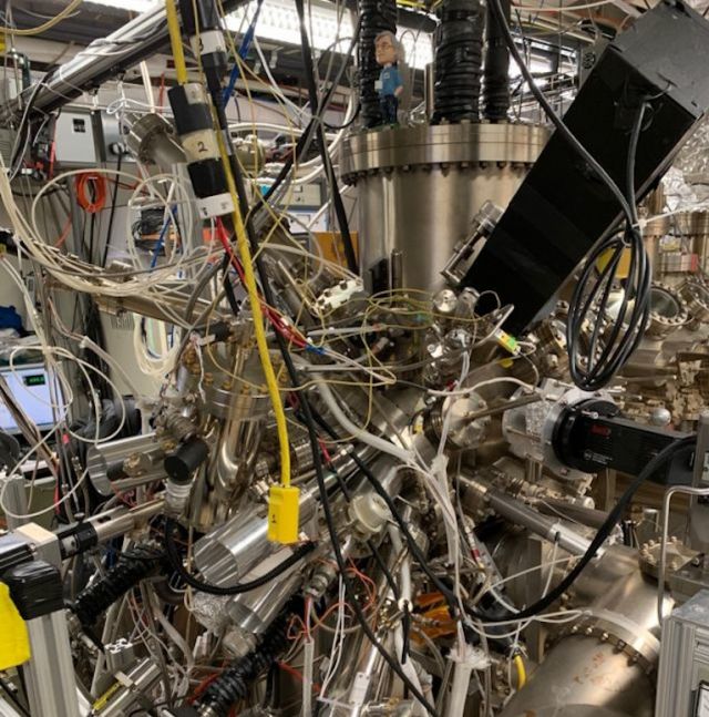
VG V80H MBE Chamber for III-V materials
-
11 effusion cells, 4 pocket e-gun
-
Pressure during growth below 3E-11 Torr
-
Prep chamber with high throughput Load-Lock and outgassing stage
-
2D: High mobility quantum well heterostructures of GaAs, InAs, InSb, InAsSb
-
1D: III-V nanowires VLS, SAG, and self assembled RE-V
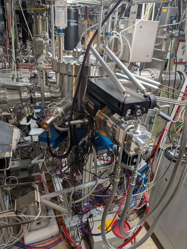
Scienta Omicron EVO 50 Cryo-MBE Chamber for Superconductors
-
Base substrate temperature below 20 K
-
8 effusion cells, 4 pocket e-gun
-
Base pressure below 4 E-11 torr
-
2.5-axis manipulator (up to 2“samples)
-
Normal to grazing angle deposition
-
Sample entry via Fast Entry Load-Lock (FEL)
-
Separate annealing stage with temperatures up to 1250 °C and hydrogen atom beam source
-
Superconducting materials Ta, Nb, Al, Mo, Ge, Bi, V, and others
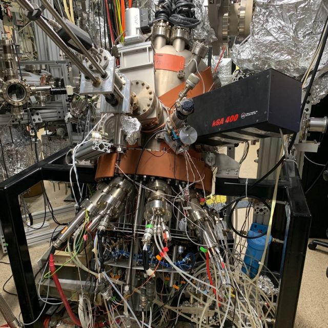
MOD Gen II EMOF MBE for Heuslers
-
8 effusion cells, single pocket e-gun
-
Magnetic materials: Co2MnAl, Co2MnSi, Fe2MnAl, Fe2MnSi, CoFe
-
Topological Materials: PtLuSb, PtLuBi, Bi, BiSb
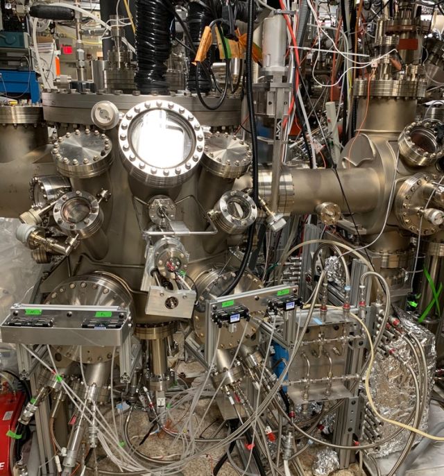
VG V80 MBE for Heuslers
-
8 effusion cells
-
Semiconducting materials: NiTiSn, CoTiSb, NiTiSb, CoFeSb
-
Topological Materials: Co2TiGe, Co2TiSn, a-Sn, SnGe
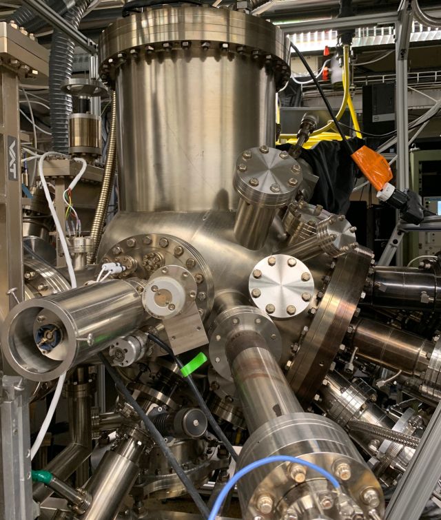
VG V80H III-V CBE
-
3 effusion cells, 1 high temperature boron cell, 13 gas lines
-
Used for growth of Phosphides and Arsenides
-
Selective area growth of nanowires
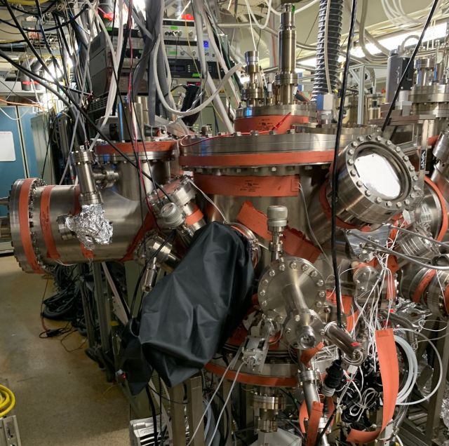
VG V80 Metal Organic MBE for Heuslers
-
4 effusion cells, 3 pocket e-gun, 4 gas lines
-
Lithium- and Magnesium-based Heuslers and half-Heuslers
-
Potentially wide-bandgap semiconductors
-
-
Prep chamber with 2 e-beam sources (currently Mo and MgO) and an outgassing stage

Veeco Chamber
-
4 effusion cells
-
Experimental materials/sources
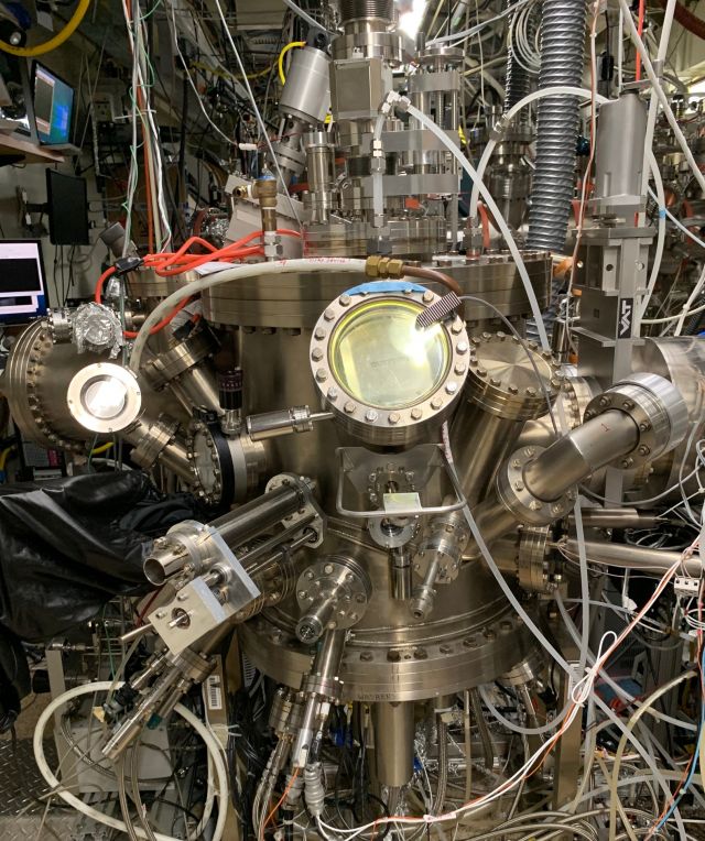
VG V80 MBE for Oxides and Nitrides
-
4 effusion cells, 3 pocket e-gun, 4 gas lines, ECR plasma source
-
2D Materials: h-BN
-
Magnetic Insulators: MnO, CuO
-
High temperature manipulator (safely up to 1200 Celsius)
"New Bi" for Superconductors
-
4 pocket e-gun, 2 effusion cells
-
Custom low-temperature substrate holder (growth at LHe or LN2 temperatures)
-
Superconductors on semiconductors
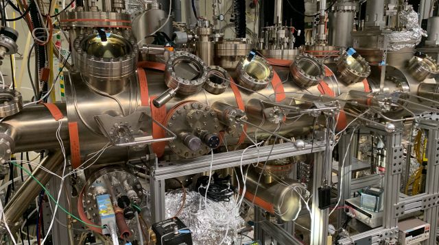
"Big Bi" for Metals and Dielectrics
-
4 pocket e-gun, 3 effusion cells
-
Capping layers and buffer layers
-
Argon sputter source for sputter-anneal cycles
-
Hydrogen cleaning for pristine surfaces
-
3" wafer bonding