Facilities
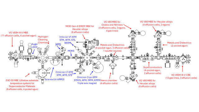
Our unique ultrahigh vacuum interconnected deposition and analysis facility allows for the growth of epitaxial metallic compounds and semiconductors by molecular beam epitaxy (MBE) and chemical beam epitaxy (CBE) techniques and characterization in-situ with scanning tunneling microscopy (STM), angle-resolved photoelectron spectroscopy (ARPES), reflection high energy electron diffraction (RHEED), low energy electron diffraction (LEED), Auger electron spectroscopy (AES) and X-ray photoelectron spectroscopy (XPS). Other analysis techniques such as Rutherford backscattering (RBS), transmission electron microscopy (TEM), atomic force microscopy (AFM) and X-ray diffraction (XRD) are used to study the grown structures.
Materials Visit Weekend 2020 Lab Tour
Materials Growth
- VG V80H MBE for III-Vs (In,Ga,Al,As,Sb) and Rare-Earths
- VG V80H CBE for III-Vs (In,Ga,Al,As,P)
- VG V80 Metal Organic-MBE for Heuslers
- VG V80 MBE for Heuslers
- VG V80 MBE for Oxides and Nitrides
- Gen II MBE for Heuslers
- VEECO Chamber for experimental sources
- 3" wafer bonding (available both in- and ex-vacuo)
- IN-DESIGN: Low Temperature MBE for superconductors
- Other various E-beam and thermal deposition sources
Materials Characterization
In-Situ
- Omicron Variable Temperature Scanning Tunneling Microscope (VT-STM) with Needle Sensor AFM
- Omicron Low Temperature STM (LT-STM) with Q-plus AFM
- Omicron Cryo-SFM with 3-axis superconducting vector magnet
- Scienta Omicron Angle-Resolved Photoelectron Spectroscopy (ARPES)
- X-ray Photoelectron Spectroscopy (XPS)
- Auger Electron Spectroscopy (AES)
- Low Energy Electron Diffraction (LEED)
- Reflection High Energy Electron Diffraction (RHEED)
- Magneto-Optic Kerr Effect (MOKE) Magnetometry
Ex-Situ
- Low and Room Temperature Photoluminescence
- Quantum Design Physical Property Measurement System (PPMS) for magneto-transport
- Quantum Design Magnetic Property Measurement System (MPMS) for SQUID Magnetometry
- HPD Adiabatic Demagnetization Refrigerator (ADR) for magneto-transport
- Mechanical Polisher for Transmission Electron Microscopy and wafer bonding
- Vacuum Suitcases for transport of surface sensitive samples without breaking UHV
Shared Use Facilities
- CNSI XRD, TEM, SEM, AFM, APT
- UCSB NanoFabrication Facility
- Various Beamlines (ALS, BESSY, SOLEIL, MAX IV)

General Lab Equipment
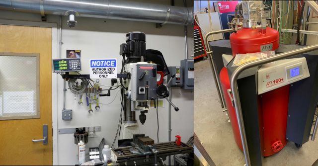
- Bench mill, saw, and grinder
- Supply of 80-20 "The Industrial Erector Set"
- Two Helium reliquifiers
- Quantum Design ATL160 reliquifies the Helium burn off from our low-temperature characterization techniques